- 您现在的位置:买卖IC网 > Sheet目录1905 > ATMEGA8HVA-4CKU (Atmel)MCU AVR 8K FLASH 4MHZ 36-LGA
143
8024A–AVR–04/08
ATmega8HVA/16HVA
26.2.1
EEPROM Write Prevents Writing to SPMCSR
Note that an EEPROM write operation will block all software programming to Flash. Reading the
Fuses and Lock bits from software will also be prevented during the EEPROM write operation. It
is recommended that the user checks the status bit (EEPE) in the EECR Register and verifies
that the bit is cleared before writing to the SPMCSR Register.
26.2.2
Setting the Lock Bits from Software
To set the Lock Bits, write the desired data to R0. If bits 1..0 in R0 are cleared (zero), the corre-
sponding Lock bit will be programmed if an SPM instruction is executed within four cycles after
RFLB and SPMEN are set in SPMCSR. The Z-pointer is don’t care during this operation, but for
future compatibility it is recommended to load the Z-pointer with 0x0001 (same as used for read-
ing the Lock bits). For future compatibility it is also recommended to set bit 7..2 in R0 to “1” when
writing the Lock bits. When programming the Lock bits the entire Flash can be read during the
operation.
See Table 27-1 on page 149 and Table 27-2 on page 149 for how the different settings of the
Lock bits affect the Flash access.
26.2.3
Reading the Fuse and Lock Bits from Software
It is possible to read both the Fuse and Lock bits from software. To read the Lock bits, load the
Z-pointer with 0x0001 and set the RFLB and SPMEN bits in SPMCSR. When an LPM instruction
is executed within three CPU cycles after the RFLB and SPMEN bits are set in SPMCSR, the
value of the Lock bits will be loaded in the destination register. The RFLB and SPMEN bits will
auto-clear 6 cycles after writing to SPMCSR if no SPM instruction is executed within four CPU
cycles. SPMCSR is locked for further writing until it is auto-cleared. The LPM instruction must be
executed within three CPU cycles after writing SPMCSR. When RFLB and SPMEN are cleared,
LPM will work as described in the Instruction set Manual.
The algorithm for reading the Fuse Low byte is similar to the one described above for reading
the Lock bits. To read the Fuse Low byte, load the Z-pointer with 0x0000 and set the RFLB and
SPMEN bits in SPMCSR. When an LPM instruction is executed within three cycles after the
RFLB and SPMEN bits are set in the SPMCSR, the value of the Fuse Low byte (FLB) will be
loaded in the destination register as shown below. Refer to Table 27-4 on page 150 for a
detailed description and mapping of the Fuse Low byte.
Fuse and Lock bits that are programmed, will be read as zero. Fuse and Lock bits that are
unprogrammed, will be read as one.
26.2.4
Preventing Flash Corruption
During periods of low V
CC, the Flash program can be corrupted because the supply voltage is
too low for the CPU and the Flash to operate properly. These issues are the same as for board
level systems using the Flash, and the same design solutions should be applied.
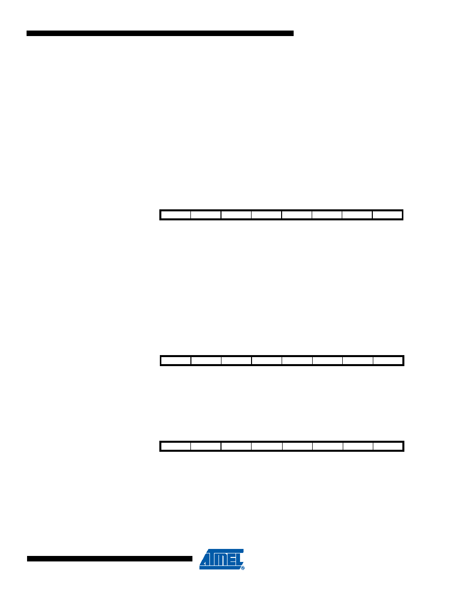
Bit
7
6
543
210
R0
11
111
1
LB2
LB1
Bit
7
6
543210
Rd
––
––––
LB2
LB1
Bit
7
65
4
3210
Rd
FLB7
FLB6
FLB5
FLB4
FLB3
FLB2
FLB1
FLB0
发布紧急采购,3分钟左右您将得到回复。
相关PDF资料
ATSAM3N4AA-AU
MCU FLASH 48-QFP
ATSAM3SD8CA-CU
IC MCU 2X256KB CORTEX-M3 100-QFN
ATSAM3U1EB-CU
IC MCU 64KB CORTEX-M3 144-TFBGA
ATSAM3X8EA-CU
IC MCU 2X256KB CORTEX-M3 144-BGA
ATTINY12V-1SUR
IC AVR MCU 1K FLASH 4MHZ 8-SOIC
ATTINY13-20SQR
IC MCU AVR 1KB FLASH 20MHZ 8SOIC
ATTINY13A-MMUR
MCU AVR 1KB FLASH 20MHZ 10DFN
ATTINY13V-10SUR
MCU AVR 1KB FLASH 10MHZ 8SOIC
相关代理商/技术参数
ATMEGA8HVA-4CKUR
功能描述:8位微控制器 -MCU AVR 8KB FLSH 512B EE 1KB SRAM - 4 MHZ RoHS:否 制造商:Silicon Labs 核心:8051 处理器系列:C8051F39x 数据总线宽度:8 bit 最大时钟频率:50 MHz 程序存储器大小:16 KB 数据 RAM 大小:1 KB 片上 ADC:Yes 工作电源电压:1.8 V to 3.6 V 工作温度范围:- 40 C to + 105 C 封装 / 箱体:QFN-20 安装风格:SMD/SMT
ATMEGA8HVA-4TU
功能描述:8位微控制器 -MCU AVR 8KB, 512B EE 4MHz 1KB SRAM 1.8-9V RoHS:否 制造商:Silicon Labs 核心:8051 处理器系列:C8051F39x 数据总线宽度:8 bit 最大时钟频率:50 MHz 程序存储器大小:16 KB 数据 RAM 大小:1 KB 片上 ADC:Yes 工作电源电压:1.8 V to 3.6 V 工作温度范围:- 40 C to + 105 C 封装 / 箱体:QFN-20 安装风格:SMD/SMT
ATMEGA8HVA-4TUR
功能描述:8位微控制器 -MCU AVR 8KB FLSH 512B EE 1KB SRAM - 4 MHZ RoHS:否 制造商:Silicon Labs 核心:8051 处理器系列:C8051F39x 数据总线宽度:8 bit 最大时钟频率:50 MHz 程序存储器大小:16 KB 数据 RAM 大小:1 KB 片上 ADC:Yes 工作电源电压:1.8 V to 3.6 V 工作温度范围:- 40 C to + 105 C 封装 / 箱体:QFN-20 安装风格:SMD/SMT
ATMEGA8HVD-4MX
功能描述:8位微控制器 -MCU AVR 8KB, 512B EE 4MHz 1KB SRAM 2.1-8V
RoHS:否 制造商:Silicon Labs 核心:8051 处理器系列:C8051F39x 数据总线宽度:8 bit 最大时钟频率:50 MHz 程序存储器大小:16 KB 数据 RAM 大小:1 KB 片上 ADC:Yes 工作电源电压:1.8 V to 3.6 V 工作温度范围:- 40 C to + 105 C 封装 / 箱体:QFN-20 安装风格:SMD/SMT
ATMEGA8L-8AC
功能描述:8位微控制器 -MCU AVR 8K FLASH 512B EE 1K SRAM ADC 3V RoHS:否 制造商:Silicon Labs 核心:8051 处理器系列:C8051F39x 数据总线宽度:8 bit 最大时钟频率:50 MHz 程序存储器大小:16 KB 数据 RAM 大小:1 KB 片上 ADC:Yes 工作电源电压:1.8 V to 3.6 V 工作温度范围:- 40 C to + 105 C 封装 / 箱体:QFN-20 安装风格:SMD/SMT
ATMEGA8L8AI
制造商:Atmel Corporation 功能描述:
ATMEGA8L-8AI
功能描述:8位微控制器 -MCU AVR 8K FLASH 512B EE 1K SRAM ADC 3V RoHS:否 制造商:Silicon Labs 核心:8051 处理器系列:C8051F39x 数据总线宽度:8 bit 最大时钟频率:50 MHz 程序存储器大小:16 KB 数据 RAM 大小:1 KB 片上 ADC:Yes 工作电源电压:1.8 V to 3.6 V 工作温度范围:- 40 C to + 105 C 封装 / 箱体:QFN-20 安装风格:SMD/SMT
ATMEGA8L-8AJ
功能描述:IC MCU AVR 8K 5V 8MHZ 32-TQFP RoHS:是 类别:集成电路 (IC) >> 嵌入式 - 微控制器, 系列:AVR® ATmega 标准包装:9 系列:87C 核心处理器:8051 芯体尺寸:8-位 速度:40/20MHz 连通性:UART/USART 外围设备:POR,WDT 输入/输出数:32 程序存储器容量:32KB(32K x 8) 程序存储器类型:OTP EEPROM 大小:- RAM 容量:256 x 8 电压 - 电源 (Vcc/Vdd):4.5 V ~ 5.5 V 数据转换器:- 振荡器型:内部 工作温度:0°C ~ 70°C 封装/外壳:40-DIP(0.600",15.24mm) 包装:管件